Via in Pad
(2020年02月24日)https://www.pcbsky.com/pcb-fabrication/via-in-pad.html
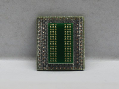
What is In Pad Via
The holes drilled on the chip pads on the PCB can be referred to as VIA IN PAD. In the manufacturing process, after the via plating, the resin is filled and then the surface is plated and filled, and the via is not visible when the patch is applied.
As we all know, via in pad technology, the PCB plugging process is a process that is produced by the higher requirements of the PCB manufacturing process and the surface mount technology.
The via hole plugging Effect has the Following Points
• Prevents short-circuiting of tin from the via through the component surface during PCB over-wave soldering
• Avoid flux remaining in the vias
• Prevent the soldering of the solder balls from over-wave soldering, causing a short circuit
• Prevent surface solder paste from flowing into the hole to cause solder joints, affecting placement
The advantage of the resin plug hole relative to the solder resist plug hole is that the flatness of the pad of the resin plug hole is higher than the flatness of the hole of the solder resist plug, and the disadvantage is high cost and complicated process.
Via in Pad: Filled with epoxy; Surface Finishing; Plated Copper Over Via.
PCBSky is a professional PCB/FPC/SMT Manufacturer in China, specializing in Quick Turn PCB & Prototypes. If you are looking for pcb shenzhen, Welcome to custom VIA IN PAD PCB directly from PCB Manufacturer China Shenzhen at low cost.
- «前のできごと |
- 次のできごと»
- このできごとのURL:


コメント