How Electron Microscopes and TOF Are Transforming Research
(2025年06月02日)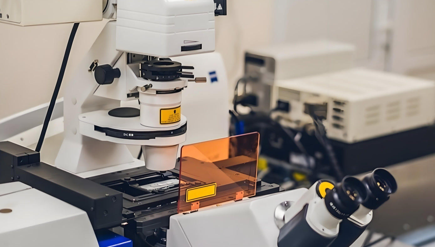
Microscopes are indispensable in scientific exploration, from studying cellular biology to analyzing advanced materials. Among the various types of microscopes, the electron microscope (EM) stands out for its unparalleled resolution and ability to reveal nanoscale structures. Compared to traditional light microscopes (LM), electron microscopes offer advanced capabilities that significantly enhance the scope and precision of scientific imaging.
This article examines the key advantages of electron microscopes over light microscopes and explores how the integration of Time-of-Flight (TOF) technology is redefining the limits of microscopic imaging and analysis.
What Are Electron Microscopes Used For?
Key Applications of Electron Microscopy
Electron microscopes use high-energy electron beams instead of visible light to image samples at extremely high resolutions. This technology is essential across many scientific disciplines, including:
Material Science
EMs are used to study the microstructure of metals, alloys, ceramics, and polymers. Scientists analyze grain boundaries, surface defects, and nanostructures with atomic precision, making EMs invaluable for materials engineering and nanotechnology development.
Biological and Cellular Research
In life sciences, electron microscopes provide detailed views of cell membranes, organelles, and even viruses. This fine-scale visualization enables better understanding of cellular processes, disease mechanisms, and molecular biology.
Medical Diagnostics and Pathology
EMs are powerful diagnostic tools in cancer research and neuroscience. They reveal ultrastructural changes in tissues and enable precise analysis of neural pathways and disease progression at the cellular level.

Semiconductor and Electronics Industry
In chip fabrication and nanoelectronics, electron microscopes are critical for inspecting wafer structures, identifying defects, and enhancing transistor performance. They play a central role in semiconductor design, testing, and quality assurance.
Nanotechnology and Advanced Materials
EMs facilitate the study of nanomaterials and nanoparticles, enabling scientists to manipulate matter at the nanoscale for applications in medicine, energy, and quantum technology.
Chemical and Elemental Analysis
Coupled with tools like Energy Dispersive Spectroscopy (EDS), electron microscopes allow researchers to conduct precise elemental composition analysis, aiding in chemical engineering, metallurgy, and environmental science.
Why Electron Microscopes Outperform Light Microscopes
1. Superior Imaging Resolution
Light microscopes are limited by optical diffraction, capping resolution at around 200 nanometers. Electron microscopes bypass this limit by using shorter electron wavelengths, achieving resolutions below 0.1 nanometers—thousands of times finer than light microscopes. This allows for the visualization of viruses, protein complexes, and atomic structures.
2. Unmatched Structural Detail
Whether examining biological tissues or industrial coatings, EMs provide high-contrast, magnified images that reveal intricate surface textures and internal features. Light microscopes simply cannot achieve this level of detail, especially at sub-cellular or nanometer scales.
3. Three-Dimensional Visualization
Advanced electron microscopes like SEM (Scanning Electron Microscope) and TEM (Transmission Electron Microscope) enable 3D imaging of microscopic samples. This adds spatial context to 2D slices, offering deeper insights into the form and function of biological and material systems.
4. Surface Composition and Analysis
Electron microscopes go beyond imaging—they analyze the elemental makeup of surfaces using EDS and other detectors. This makes EMs a dual-purpose tool for both visualization and compositional analysis, which is not possible with standard light microscopes.
The Game-Changer: Integrating Time-of-Flight (TOF) Technology with Electron Microscopy
Time-of-Flight (TOF) technology measures the time it takes for particles or photons to travel between two points. Widely used in LiDAR, depth-sensing cameras, and autonomous systems, TOF’s precision and real-time data capabilities make it a powerful enhancement for electron microscopy.

1. Bringing Depth to High-Resolution Imaging
Traditional EMs capture high-detail 2D images but lack depth perception. With TOF integration, electron microscopes can reconstruct 3D spatial data by measuring reflected signal delays. This enables comprehensive 3D imaging of microstructures, ideal for studying complex cells, layered materials, or nanoscale devices.
2. Faster, More Accurate Imaging
TOF systems enhance the imaging speed of electron microscopes by rapidly collecting flight time data, enabling quicker scans with reduced distortion. This is especially valuable when analyzing large biological tissues or extended semiconductor surfaces where time efficiency and accuracy are critical.
3. Enhanced Biomedical Insight
TOF-enhanced electron microscopes enable early disease detection by providing both structural detail and depth measurements of abnormal cells. In oncology, this can mean earlier identification of cancerous tissues. In neuroscience, it allows mapping the three-dimensional connections between neurons with greater fidelity.
4. Nanotechnology and Semiconductor Breakthroughs
For semiconductors, TOF technology reveals fine internal variations—such as microcracks or subsurface voids—that conventional EMs might miss. In nanotechnology, this integration enables 3D modeling of nanoscale devices, improving material design, chip reliability, and product innovation.
Conclusion
Electron microscopes are foundational to scientific discovery, providing nanometer-scale resolution and critical structural insights across biology, materials science, and engineering. Their capabilities far surpass those of light microscopes, offering unparalleled clarity, 3D imaging, and elemental analysis.
By integrating Time-of-Flight (TOF) technology, electron microscopes are entering a new era of advanced 3D visualization, rapid data acquisition, and real-time spatial analysis. This synergy is transforming research across disciplines—accelerating breakthroughs in medicine, driving innovation in semiconductor manufacturing, and pushing the boundaries of nanotechnology.
As TOF and electron microscopy technologies continue to evolve, their combined impact promises a future of smarter, faster, and more precise scientific tools—powering the next wave of discoveries in the microscopic world.
Synexens 3D Of RGBD ToF Depth Sensor_CS30
SHOP NOWhttps://tofsensors.com/collections/time-of-flight-sensor/products/rgbd-3d-camera
After-sales Support:
Our professional technical team specializing in 3D camera ranging is ready to assist you at any time. Whether you encounter any issues with your TOF camera after purchase or need clarification on TOF technology, feel free to contact us anytime. We are committed to providing high-quality technical after-sales service and user experience, ensuring your peace of mind in both shopping and using our products.
- このできごとのURL:


コメント