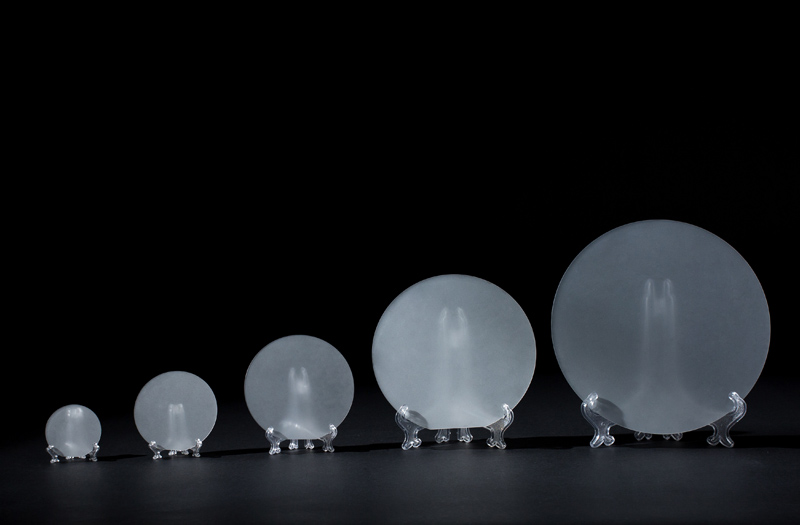
PROCESSING TECHNOLOGY OF LED PATTERNED SAPPHIRE SUBSTRATE
(2021年04月27日)For patterned sapphire substrate, before it becomes a qualified substrate, it has gone through several processes, such as cutting, rough grinding, fine grinding and polishing. Take 2-inch sapphire as an example:
1. Cutting: Cutting is made from sapphire crystal rod with a wire cutting machine, and the thickness is about 500um. In this process, the diamond wire saw is the most important consumables, which are mainly from Japan, South Korea and Taiwan.
2. Rough polishing: The surface of sapphire is very rough after cutting, which is needed to repair deep scratch and improve the overall flatness. In this step, B4C (50 ~ 80um) and coolant is used for grinding. After grinding, the surface roughness Ra is about 1um.
3. Finish polishing: The next step is fine processing, because it is directly related to the yield and quality of the final product. At present, the thickness of the standardized 2-inch patterned sapphire substrates is 430um, so the total removal amount of fine polishing is about 30um. Considering the removal rate and the final surface roughness Ra, polycrystalline diamond solution and resin tin plate are used to process in lapping mode.
4. Polishing: Although the scratch caused by polycrystalline diamond is obviously smaller than that of a single-crystal diamond, it will still leave obvious scratches on the surface of sapphire. Therefore, it will be polished by CMP to remove all scratches and leave a perfect surface. The CMP technology was originally used to flatten silicon substrate, but now it is also applicable to patterned sapphire substrate. After the CMP polishing process of the sapphire substrate after layer testing, qualified products can be handed over to the epitaxial factory for epitaxy.
CRYSCORE OPTOELECTRONIC LIMITED is a professional sapphire wafers manufacturer. We provide Sapphire Wafers, Sapphire Windows and so on. Want to know about sapphire optics? Please contact us.
- このできごとのURL:


コメント