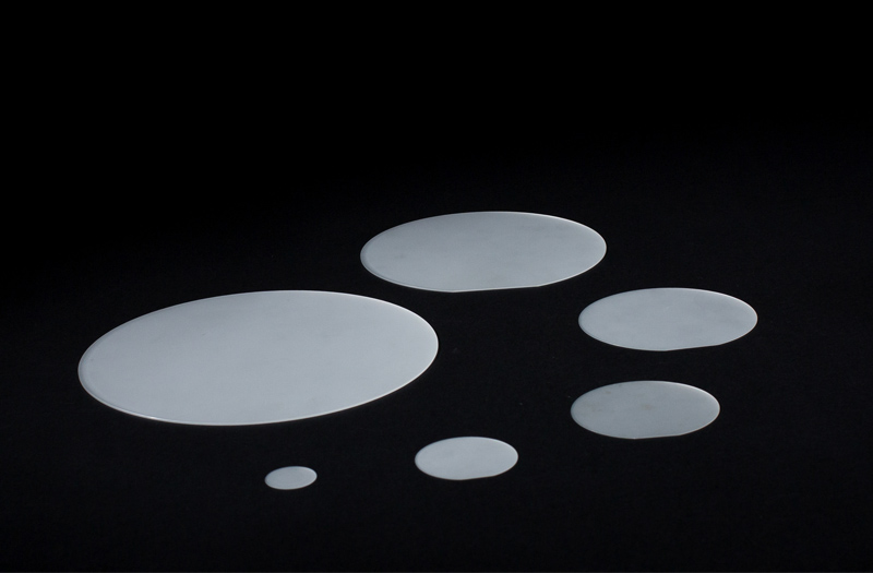
PATTERNED SAPPHIRE SUBSTRATE
(2021年04月23日)https://www.cryscore.com/led-substrates.html
PSS, namely Patterned Sapphire Substrate, refers to the preparation of periodic patterned structure on Sapphire Substrate, which is a technology developed in recent years to effectively improve the light output efficiency of LED chips. The patterned interface changes the growth process of GaN, which can reduce the dislocation defects of the GaN epitaxy and improve quantum efficiency. In addition, the rough GaN/sapphire interface can scatter the photons emitted from the source area, so that the originally fully reflected photons have the opportunity to be emitted out of the device, to effectively improving the light-extraction efficiency. Therefore, LED using PSS technology can greatly improve the luminous intensity and luminous efficiency compared with ordinary LED, also the reverse leakage current can be reduced and the life of LED devices can be extended.
Sapphire substrate can be divided into the micron-scale sapphire substrate and the nanoscale sapphire substrate according to the lattice constant. The nanoscale sapphire substrate has band-gap effects on photonic crystals that are not present in micron-scale substrates. The banding effect peculiar to the photonic crystal can be used to control the photons so that more photons can be emitted to the outside of the LED without being absorbed by the substrate. It proves that the performance of LED can be improved by using a nanoscale patterned sapphire substrate than a micro-scale one.
The main preparation technology of PSS includes wet etching and dry etching.
Wet etching:
1. Depositing SiO2 on the sapphire substrate using the plasma-enhanced chemical vapor deposition (PECVD) or daub photo-resist mask.
2. Transfer the pattern to the mask using lithography.
3. Using mixed acid solution (H3PO4 and H2SO) for corrosion, under the protection of mask.
4. After removing the mask on the surface, we can get the PSS.
Dry etching:
1. Depositing SiO2 on the sapphire substrate using the plasma-enhanced chemical vapor deposition (PECVD) or daub photo-resist mask.
2. Make Lithographic pattern on the mask by using the Lithography technique:
Firstly, the etched gas will be glow-discharge and generate active particles by inductive coupling, which interact with the solid surface of the substrate.
3. After removing the mask on the surface, we can get the PSS.
LED sapphire substrate is very important, if you are looking for related products, contact us to get a quote.
CRYSCORE OPTOELECTRONIC LIMITED is a professional sapphire wafers manufacturer. We provide Sapphire Wafers, Sapphire Windows, Al2O3 substrate and so on. Want to know about optical sapphire? Please contact us.
- このできごとのURL:


コメント