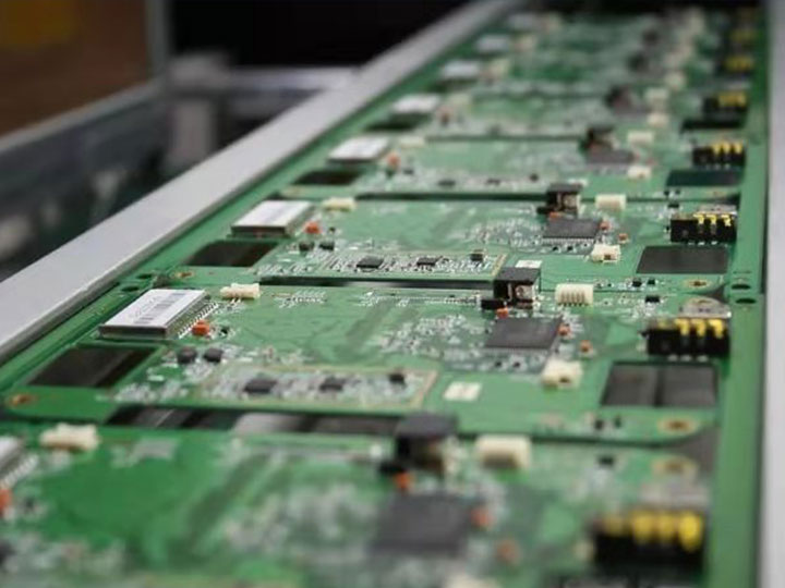
How to Improve PCB Design of Bluetooth Circuit Boards?
(2023年06月02日)https://www.hx-technology.com/products/
Ⅰ. Bluetooth circuit board design guide
If certain precautions are not taken, PCBs with Bluetooth technology may experience interference, data loss, and poor signal integrity. We will outline many of the rules and guidelines to consider when choosing Bluetooth technology for a specific application, especially when designing it into a circuit board.
Various applications utilizing Bluetooth circuit boards include: beacons used in shopping malls; eddy current frames for industrial sensing applications; headsets and audio, stereo products; remote peripherals such as video game controllers or computer mice, keyboards; home automation systems; wireless consumer electronics applications, including cameras, printers and telephones.
Bluetooth technology is more than 20 years old and is still evolving, and although Bluetooth technology has improved in speed, power, range, security and other attributes over the years, it seems to have remained since its inception in the mid-90s. Some of the same issues, including its susceptibility to signal interference. So, from a PCB design perspective, what can be done to optimize signal integrity and minimize interference and lost packets?
Ⅱ. How to improve the PCB design of the Bluetooth green circuit board
1. Use certified modules
If integrating Bluetooth into a product and resources are limited, consider using a pre-certified, fully-contained module to help speed development and time-to-market. It might end up adding a little cost, but usually avoid some of the hassle of antenna placement, design, and EMI susceptibility.
2. Check the Bluetooth device selection
Make sure the proper Bluetooth device is selected for the Bluetooth PCB and the antenna is properly sized and adjusted. If you want to use a simple beacon application that only needs short bursts, intervals to announce location or data, a low power, cost-effective solution with minimal functionality and peripherals can be used to save costs.
3. Separation or removal of copper signals and high-energy components
When designing a Bluetooth PCB, keep the antenna area completely away from nearby copper signals or components that carry a lot of energy.
4. Notes on power supply
Make sure the rails that power the Bluetooth module or chip are clean, and use bypass and decoupling capacitors if needed. It is also possible to use ferrite beads on the power rails into the Bluetooth area of the board to suppress high frequency noise.
5. Tools and analysis
If you are designing an antenna area, make sure you have the proper equipment to analyze and tune the matching network, or consider sending your design to a third-party RF test lab.
As a pcb assembly company, we will do our best to meet all the needs of customers.
- このできごとのURL:


コメント