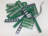
Have You Neglected The Design Of Solder Pad In PCB Board Design?
(2021年)http://www.kom-key.com/graphic-overlay/
http://www.kom-key.com/graphic-overlay/
http://www.kom-key.com/how-to-fix-the-membrane-switch-if-broken.html
Komkey,a membrane switches supplier, is a pioneer in the graphic overlay manufacturers of custom membrane keypad, graphics, nameplate, label, dispensing glue and touch panel, we have gathered over 10 years of experience in the field which guarantee our customers deliver date, top-highly quality, favorable price, excellent customer service, and quick reply.
When designing PCB pad in PCB board design, it is necessary to design in strict accordance with relevant requirements and standards. Because in SMT chip processing, the design of PCB pads is very important. Pad design will directly affect the weldability, stability and heat transfer of components, and affect the quality of chip processing. So what is the standard of PCB pad design?
I Design standards for the shape and size of PCB pads
1. Call the PCB standard packaging library.
2. The minimum of one side of all pads is not less than 0.25mm, and the maximum diameter of the entire pad is not more than 3 times the component aperture.
3. Try to ensure that the distance between the two pad edges is greater than 0.4mm.
4. Pads with aperture over 1.2mm or pad diameter over 3.0mm shall be designed as diamond or quincunx pads;
5. In case of dense wiring, it is recommended to use elliptical and oblong connecting disks. The diameter or minimum width of the single panel pad is 1.6mm. The double-sided weak current circuit pad only needs to increase the hole diameter by 0.5mm, because if the pad is too large, it is likely to cause unnecessary continuous welding.
II PCB pad via size standard
In general, the inner hole of the pad is not less than 0.6mm, because the hole less than 0.6mm is not easy to be processed when the die is getting punched. Under normal circumstances, the diameter of the metal pin plus 0.2mm is used as the inner hole diameter of the pad. For example, when the diameter of the metal pin of the resistance is 0.5mm, the inner hole diameter of the pad corresponds to 0.7mm. The diameter of the pad depends on the inner hole diameter.
III Key points for reliability design of PCB pads
1. Symmetry. In order to ensure the balance of the surface tension of the molten solder, the pads at both ends must be symmetrical.
2. Pad pitch. Too large or too small pad pitch can cause welding defects, so make sure that the component tip or lead is properly spaced from the pad.
3. Remaining pad size. The remaining dimensions of the component heads or pins after bonding to the pads must ensure that the solder joints can form a meniscus.
4. Pad width. It should be basically the same as the width of the component tip or pin.
The correct pad design of PCB can be corrected due to the effect of surface tension of molten solder during reflow soldering if there is a small amount of skew during chip processing. However, if the PCB pad design is not correct, even if the mounting position is very accurate, the component position deviation, suspension bridge and other welding defects are easy to appear after reflow welding. Therefore, when designing PCB pad, great attention should be paid.
Our company provide many service,which include graphic overlay membrane,for example membrane switches graphic overlays,graphic overlay prototype,graphic overlay as will as how to fix a membrane keyboard, If you have interest about our servicer,you can contact us anytime you want.
- このできごとのURL:


コメント